Researchers build 2D MoS2 transistors using coal-derived carbon dot dielectrics
Engineers used coal-derived carbon dots as a seed layer for atomic layer deposition, creating gate dielectrics with a 0.6-nanometre equivalent oxide thickness.
Engineers from the University of Illinois Urbana-Champaign and the National Energy Technology Laboratory have demonstrated top-gated two-dimensional transistors using carbon nanodots derived from bituminous coal, according to nature.com nature.com
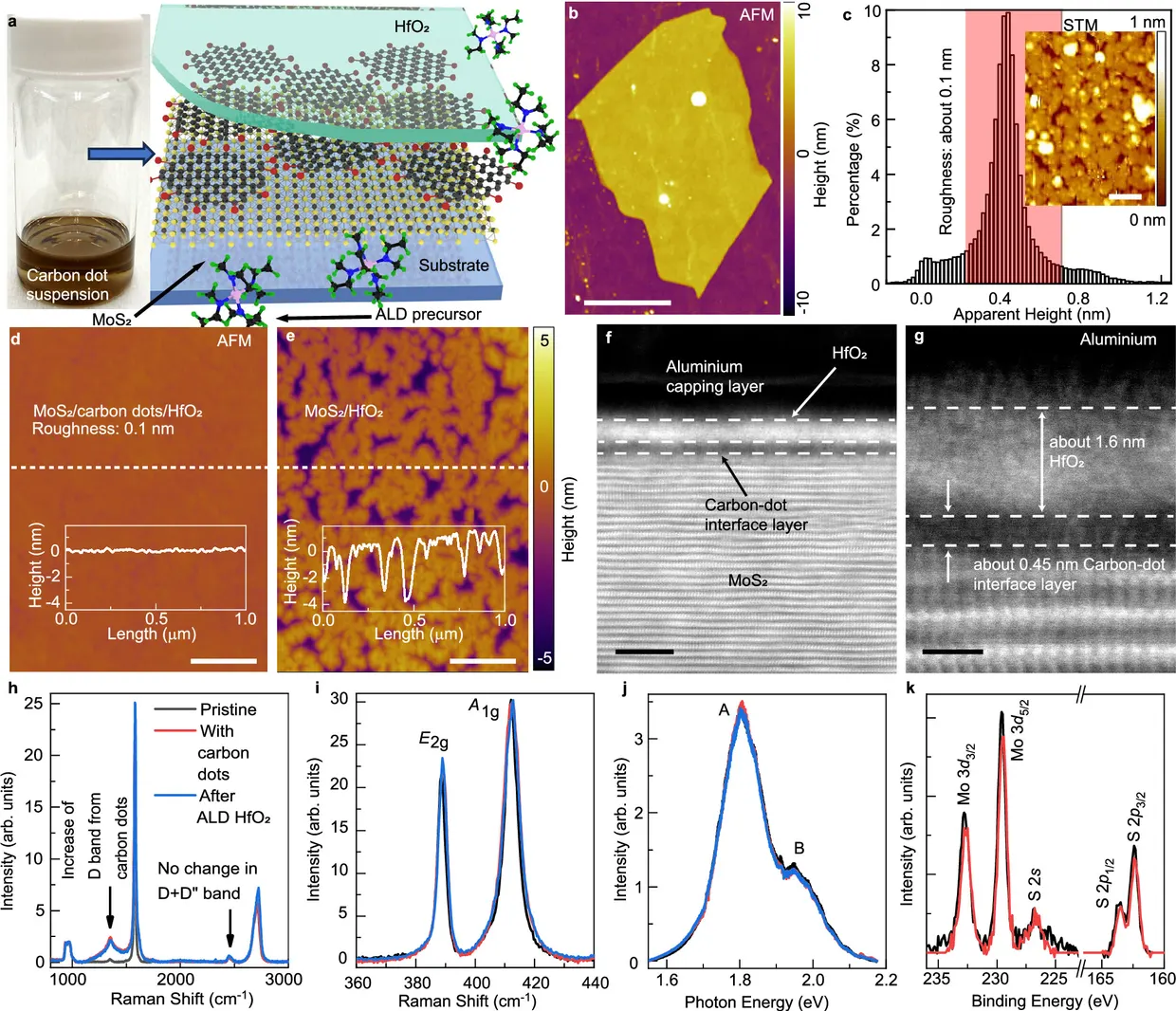
nature.comnature.comOpen source ↗. The researchers assembled these graphene-like dots into an atomically thin nucleation layer for the atomic layer deposition of hafnium dioxide onto molybdenum disulfide (MoS2) and graphene channels. The resulting hybrid dielectric reached an equivalent oxide thickness (EOT) of 0.6 ± 0.1 nm, a leakage current density below 10⁻⁴ A·cm⁻², and a breakdown field of 28 MV·cm⁻¹.
Interfacial assembly and dielectric performance
Direct growth of high-κ gate dielectrics on two-dimensional materials is typically hindered by their chemically inert van der Waals surfaces, which lack dangling bonds to serve as nucleation centers. Conventional seed layers often cause high interfacial roughness, decompose below 220 °C, or damage the underlying 2D channel. To bypass these issues, the team applied carbon dots measuring 1 to 5 nm in diameter and approximately 0.4 nm in thickness from solution dispersions under mild conditions. The carbon dots assembled into a dense monolayer that binds non-covalently without chemical hybridization, providing a thermal stability of at least 400 °C.
Transistor characteristics and low-voltage logic
Top-gated MoS2 field-effect transistors built with the carbon dot/HfO2 dielectric bilayer showed a subthreshold swing approaching the thermionic limit of 60 mV·dec⁻¹ and a hysteresis below 30 mV. The devices exhibited near-zero positive threshold voltages for enhancement-mode operation, with a narrow threshold distribution of 60 mV and bias-stress drift under 25 mV. Leveraging this sub-nanometre EOT and interface stability, the authors fabricated multi-transistor logic circuits operating at a supply voltage of 0.5 V.