Full-size 3D-printed tungsten tiles endure 74 plasma pulses in DIII-D tokamak
Engineers from NC State, ORNL, and JEOL manufactured full-scale divertor tiles via electron-beam 3D printing and verified their stability under high heat flux.
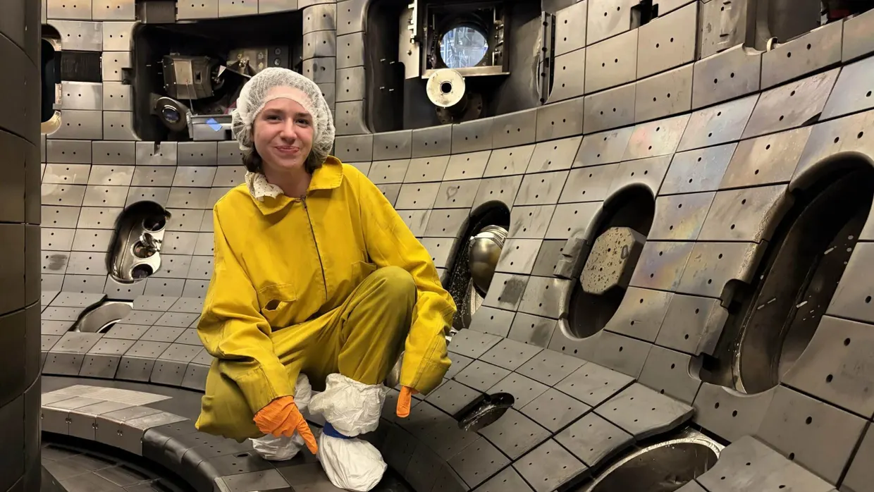
A research collaboration involving North Carolina State University, Oak Ridge National Laboratory (ORNL), and JEOL Ltd. has fabricated full-size tungsten tiles and tested them in the DIII-D National Fusion Facility in San Diego, according to engr.ncsu.edu engr.ncsu.edu
engr.ncsu.eduengr.ncsu.eduOpen source ↗. The additively manufactured divertor components endured 74 direct plasma discharges with significant heat and particle flux without structural failure. The hardware transition from program invitation to installation in the tokamak took approximately eight months.
Powder bed fusion above ductile-to-brittle transition
Tungsten possesses the highest melting point of any metal at 3,422 °C and a density of 19.3 grams per cubic centimeter, making it the primary material candidate for divertor armor in tokamaks such as ITER. However, conventional machining and casting remain difficult due to its ductile-to-brittle transition temperature, which falls between 200 °C and 600 °C, causing crack formation during laser-based printing processes. To resolve thermal stress fractures, the team utilized electron-beam powder bed fusion (EB-PBF) inside a vacuum chamber. The rapid scanning capabilities of the electron beam maintained the surrounding powder bed at temperatures above 1,400 °C throughout fabrication, keeping the metal well above its brittle range and yielding dense, crack-free components.
Fabrication and in-vessel testing
JEOL engineered and printed the full-scale tiles on a large-format EB-PBF system in Japan, ORNL provided fusion materials expertise and funding, and NC State directed final machining, tight-tolerance finishing, and material characterization. The divertor tiles are designed to operate in tokamak exhaust zones where steady-state heat loads reach 10 to 20 megawatts per square meter. The campaign follows earlier Divertor Materials Evaluation System (DiMES) tests at DIII-D, where printed tungsten specimens handled heat fluxes approaching 20 megawatts per square meter, with peak pulses exceeding 35 megawatts per square meter, confirming baseline performance prior to full-tile deployment.